Crystals in Nanofocus
Max Planck Scientists strike new paths in nanoanalysis and data storage with infrared light
Scientists of the Nano-Photonics Group at the Max Planck Institute of Biochemistry have developed a new infrared-optical nanotechnology based on the excitation of lattice vibrations in polar crystals (phonons). The technology, called "phonon photonics", opens up entirely new applications of infrared light: non-destructive chemical and structural analysis of crystals at a resolution better than 1/10000 mm, infrared data storage providing storage densities better than DVD, nanoscopic infrared-sensors or waveguides and switches for the development of future infrared-optical supercomputers. The physicists in Martinsried present their initial studies on silicon carbide crystals in the latest issue of NATURE MATERIALS (Nature Materials, September 2004, published online 1 August 2004).
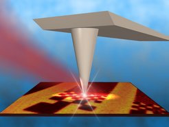
 intensifies the illuminating infrared light from a CO2 laser at its tip to a tiny spot of only few 10 Nanometer diameter. The antenna is scanning the surface of of a silicon carbide (SiC) crystal in which a checkerboard pattern was implanted by a Ga+-beam. The scattered light from the antenna is measured and allows the damage areas to be identified by a strongly reduced intensity of the scattered light. In the infrared image the undamaged areas thus appear bright and the damaged areas appear dark. The size of the checkerboard squares varies between 200 Nanometer and 1.6 Micrometer, which is much smaller than the wavelength of the infrared light (about 10 Micrometer).")
The spatial resolution in microscopy and lithography as well as the storage density in optical data storage is limited to the wavelength of the light used, i.e several hundreds of nanometers (1 nanometer = 1 millionth of a millimeter). In recent developments, the resolution is improved by using light of ever shorter wavelengths (UV-light). Rainer Hillenbrand and his colleagues at the Max Planck Institute of Biochemistry, however, have developed an optical nanotechnology based on particularly long wavelengths, namely infrared respectively thermal radiation.
Infrared light is particularly interesting as it allows the analysis of a material´s chemical composition and it´s crystal structure. Thus, infrared spectroscopy is a widely used analytical tool in material sciences, biochemistry and biomedicine. Unfortunately the long wavelengths limit the spatial resolution of infrared spectrometers and microscopes to several micrometers. Therefore nanometer-scale resolved chemical and structural mapping of materials is impossible with conventional techniques. The nanometer scale is, however, of crucial relevance to biological structures such as cell membranes and to novel nanocomposite materials.
Over the last years scientists at the Max Planck Institute of Biochemistry in Martinsried near Munich have been developing a totally new microscopy technique that achieves a resolution independent of the illumination wavelength. Their so-called near-field microscope uses an extremly sharp needle that scans a surface and thereby focuses the incoming light 300-times better than any optical lens can do. Two years ago the scientists demonstrated that this "nanofocused" infrared light can excite local lattice vibrations in polar crystals (Nature 418, 159-162 (2002); press release of the Max Planck Society "Infrared antenna for nano-size mapping, July 19th, 2002"). Depending on the crystal´s chemical and structural composition, specific wavelengths are needed that represent an "infrared fingerprint" of the crystal. Already in 2002, the physicists announced fascinating applications of their infrared nanoscope for non-destructive characterization of crystal surfaces and for optical data storage.
In the most recent issue of "Nature Materials" Nenad Ocelic and Rainer Hillenbrand now present the experimental proof that their near-field microscope indeed allows nanoscale mapping of crystal quality by infrared excitation of local lattice vibrations. The near-field microscope thereby reaches a 100-fold higher resolution compared to conventional infrared microscopes. By focused ion beam implantation the scientists induced controlled lattice damage at the surface of a silicon carbide (SiC) crystal. On the locally damaged parts of the crystal the infrared excitation is dramatically reduced. The strongly reduced brightness in the infrared images thus allows them to identify the damaged areas. As the near-field microscopy technique is non-destructive, it is well suited not only for basic materials research but also for quality control in crystal growth or wafer production in the semiconductor industry.
The results also open new and unexpected perspectives for optical data storage. The smallest bits that were fabricated and detected by the scientists are 100 times smaller than the wavelength of infrared light. Despite this, the near field microscope enables them to be mapped with extraordinary sharpness. Although the wavelength of the infrared light used is 20 times longer than visible wavelengths (used for optical data reading), the Max Planck researchers already achieved storage densities beyond that of DVD. For silicon carbide, e.g. used as an abrasive grit, data encoding by lattice damage is physically, chemically and thermally extremely stable: The method could be used for long-term archival data storage. "By further optimizing our technique storage densities of up to 1 Terabit/cm2 should be possible," says Rainer Hillenbrand, head of the independent junior research group.
Potential applications of coupling light (photons) to lattice vibrations in polar crystals (phonons) go even further: Infrared light could be nanofocused, manipulated and detected by nanocrystals or nanostructured crystal surfaces. Hillenbrands group is spotting applications of the technology - called phonon-photonics - in tiny infrared sensors useful for detecting the smallest amounts of chemical or biological substances, e.g. for highly sensitive medical diagnostics. In addition to analytical applications, coupling of light to nanostructured crystals could allow the realization of nanoscale waveguides for infrared and terahertz waves that could lead to extremly small circuits for infrared-optical information processing (infrared-optical computer).
With his concept of "phonon-photonics" Rainer Hillenbrand was awarded financial support within the young scientist competition in nanotechnology announced by the Federal Ministry of Education and Science (Bundesministerium für Bildung und Forschung, BMBF) in 2002. The BMBF is supporting Hillenbrand’s independent junior research group at the Max Planck Institute of Biochemistry over a 5 years period.